Printed Circuit Boards (PCBs) are the backbone of modern electronic devices, from simple household gadgets to sophisticated space technology. Understanding the intricate process of how PCBs are made is not only fascinating but also essential for anyone involved in electronics design and manufacturing. This comprehensive guide will take you through every step of PCB manufacturing, highlighting key processes, materials, and technologies involved.
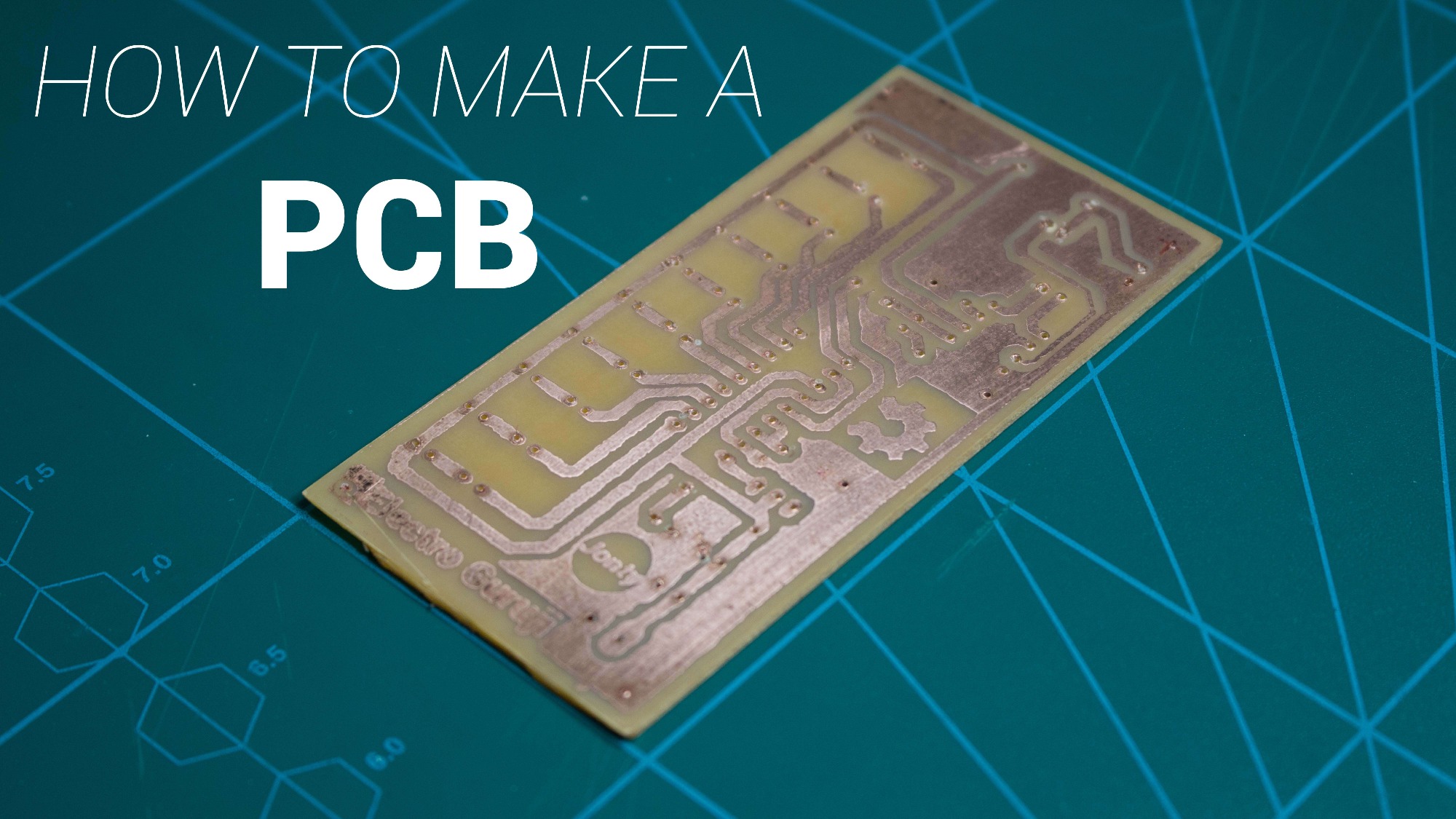
Table of Contents
- Introduction to PCBs
- Designing a PCB
- Materials Used in PCB Manufacturing
- PCB Manufacturing Process
- PCB Design and Layout
- Printing the PCB Design
- Etching the PCB
- Drilling
- Plating
- Solder Mask Application
- Silkscreen Application
- Surface Finish
- Electrical Testing
- Types of PCBs
- Applications of PCBs
- Conclusion
Introduction to PCBs
A Printed Circuit Board (PCB) mechanically supports and electrically connects electronic components using conductive tracks, pads, and other features etched from copper sheets laminated onto a non-conductive substrate. They are the foundation of most electronic devices, enabling complex circuitry to be embedded in compact spaces.
Designing a PCB
The design process is the first and most crucial step in PCB manufacturing. It involves creating a blueprint that outlines the board's layout, including the placement of components and routing of electrical connections. Here's a breakdown of the key stages in PCB design:
- Schematic Capture: This step involves creating a schematic diagram that represents the electrical connections between components.
- Component Placement: Designers place components on the board, considering factors like signal integrity, thermal management, and manufacturability.
- Routing: This involves drawing the electrical connections between components. Routing can be single-layer, double-layer, or multi-layer, depending on the board's complexity.
- Design Rule Check (DRC): A DRC is performed to ensure the design adheres to manufacturing constraints and standards.
Materials Used in PCB Manufacturing
Several materials are used in PCB manufacturing, each serving a specific purpose:
- Substrate (Base Material): Typically made of fiberglass-reinforced epoxy resin (FR4), the substrate provides the mechanical support for the board.
- Copper Foil: Thin sheets of copper are laminated onto the substrate to form the conductive pathways.
- Solder Mask: This is a protective layer applied over the copper traces to prevent short circuits and oxidation.
- Silkscreen: Used to print text and symbols on the board, aiding in component identification and assembly.
- Surface Finish: Various finishes, such as HASL (Hot Air Solder Leveling), ENIG (Electroless Nickel Immersion Gold), and OSP (Organic Solderability Preservative), are applied to protect the exposed copper and enhance solderability.
PCB Manufacturing Process
The PCB manufacturing process is intricate and involves several precise steps:
1. PCB Design and Layout
The process begins with designing the PCB layout using specialized software like Eagle, Altium Designer, or KiCad. The layout includes the positioning of components and the routing of electrical connections. Once finalized, the design is exported as Gerber files, which are standard file formats used in PCB manufacturing.
2. Printing the PCB Design
The Gerber files are used to print the PCB design onto a photoresist film. This film is a crucial part of the photolithography process, where UV light is used to transfer the design onto the copper-clad laminate.
3. Etching the PCB
In the etching process, the unprotected copper areas (those not covered by the photoresist) are removed using a chemical solution, typically ferric chloride or ammonium persulfate. This leaves behind the desired copper traces that form the electrical pathways.
4. Drilling
Precision drilling machines create holes for through-hole components and vias (vertical interconnect accesses) that connect different layers of the PCB. Laser drilling is often used for high-density interconnects (HDI) to achieve smaller hole sizes.
5. Plating
After drilling, the board undergoes a plating process to coat the walls of the drilled holes with copper, forming electrical connections between different layers of the PCB. Electrolytic and electroless plating methods are commonly used.
6. Solder Mask Application
A solder mask is applied to the board to insulate and protect the copper traces from oxidation and short circuits. The solder mask also prevents solder bridges during component soldering. It is typically applied using a silkscreen printing process or a photoimageable method.
7. Silkscreen Application
The silkscreen layer is applied to the PCB to print text, component outlines, logos, and other identifiers on the board. This helps in assembly and debugging. The silkscreen is usually applied using a screen-printing process.
8. Surface Finish
Various surface finishes are applied to the PCB to protect the exposed copper and improve solderability. Common finishes include HASL, ENIG, OSP, and immersion tin/silver. The choice of finish depends on the application, cost, and desired shelf life.
9. Electrical Testing
Before the PCBs are shipped, they undergo rigorous electrical testing to ensure there are no shorts or open circuits. Automated test equipment (ATE) is used to check continuity and isolate faults.
Types of PCBs
PCBs come in various types, each suited for different applications:
- Single-Sided PCBs: These have a single layer of copper on one side of the board. They are simple and cost-effective but limited in complexity.
- Double-Sided PCBs: These have copper layers on both sides of the board, allowing for more complex circuitry and connections.
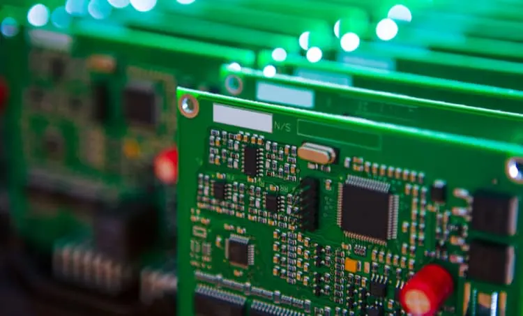
- Multi-Layer PCBs: These consist of multiple layers of copper separated by insulating material, enabling highly complex and dense circuit designs.
- Flexible PCBs: Made from flexible materials, these boards can bend and fold, making them ideal for dynamic or constrained spaces.
- Rigid-Flex PCBs: A combination of rigid and flexible boards, these offer the benefits of both types, often used in advanced applications like aerospace and medical devices.
- High-Frequency PCBs: Designed for high-speed applications, these boards use special materials to minimize signal loss and impedance issues.
Applications of PCBs
PCBs are integral to virtually every electronic device. Here are some of their primary applications:
- Consumer Electronics: Smartphones, tablets, laptops, and home appliances all rely on PCBs for their operation.
- Medical Devices: PCBs are used in medical imaging equipment, pacemakers, and diagnostic devices, where reliability and precision are paramount.
- Automotive Industry: Modern vehicles use PCBs in engine control units, infotainment systems, and advanced driver-assistance systems (ADAS).
- Aerospace and Defense: PCBs are used in navigation, communication, and control systems, where they must withstand extreme conditions.
- Industrial Equipment: Manufacturing and automation equipment rely on PCBs for control and monitoring systems.
- Telecommunications: PCBs are vital in networking equipment, including routers, switches, and base stations, facilitating data communication.
Conclusion
The manufacturing of PCBs is a complex and meticulous process, involving multiple steps and various materials. From the initial design phase to the final testing, each stage is critical in ensuring the reliability and functionality of the final product. Understanding how PCBs are made provides valuable insights into the electronics industry, highlighting the importance of precision and quality in creating the electronic devices we rely on every day.
By grasping the intricacies of PCB manufacturing, designers, engineers, and enthusiasts can appreciate the technology's role in modern electronics and contribute to its continual advancement.


![[KES 2025] Zero One Solution Limited to Showcase Advanced PCBA Solutions at KES 2025 in Seoul](http://ueeshop.ly200-cdn.com/u_file/UPAY/UPAY381/2510/photo/ae5b6fdca5.jpg)

