The PCB (Printed Circuit Board) assembly process is a critical aspect of electronics manufacturing, involving various stages from placing components on the board to ensuring the final product works as intended. This guide provides an in-depth look into each step of the PCB assembly process, aiming to offer clarity and insight for both seasoned professionals and newcomers. Whether you’re looking to improve your understanding or optimize your production process, this comprehensive guide covers everything you need to know.
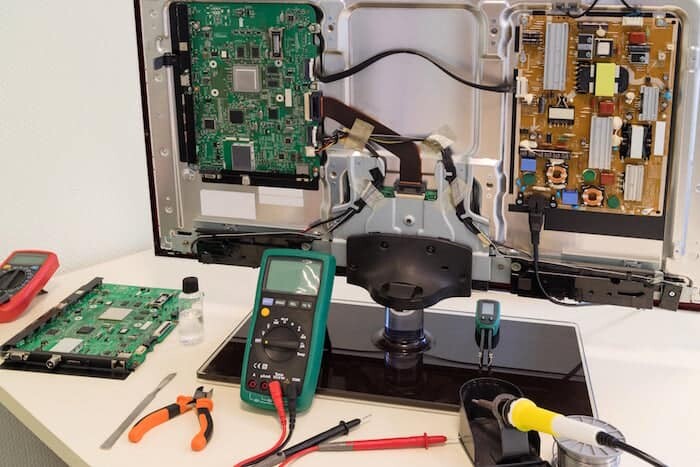
Table of Contents
- Introduction to PCB Assembly
- Component Procurement
- Solder Paste Application
- Pick and Place
- Reflow Soldering
- Inspection and Quality Control
- Through-Hole Component Insertion
- Wave Soldering
- Final Assembly and Testing
- PCB Assembly Tools and Equipment
- Challenges in PCB Assembly
- Future Trends in PCB Assembly
- Conclusion
Introduction to PCB Assembly
PCB assembly (PCBA) is the process of mounting and soldering electronic components onto a PCB to create a functional circuit board. The process can involve various methods and technologies, depending on the complexity and requirements of the board.
Key Steps in PCB Assembly
- Component Procurement: Sourcing all necessary components for the assembly.
- Solder Paste Application: Applying solder paste to the PCB pads.
- Pick and Place: Placing components onto the PCB.
- Reflow Soldering: Soldering the components to the PCB.
- Inspection and Quality Control: Ensuring the assembled PCB meets quality standards.
- Through-Hole Component Insertion: Inserting and soldering through-hole components.
- Wave Soldering: Soldering through-hole components using wave soldering.
- Final Assembly and Testing: Completing assembly and testing the PCB for functionality.
Component Procurement
Component procurement is the first step in the PCB assembly process. It involves sourcing all necessary electronic components, ensuring their quality and compatibility with the PCB design.
Best Practices for Component Procurement
- Supplier Selection: Choose reliable suppliers with a track record of delivering quality components.
- Component Verification: Verify component specifications and compatibility with the PCB design.
- Inventory Management: Maintain an organized inventory to avoid shortages and delays.
- Cost Management: Balance cost and quality to stay within budget without compromising on performance.
- Lead Time Management: Plan procurement timelines to align with production schedules.
Solder Paste Application
Solder paste application involves depositing solder paste onto the PCB pads where components will be placed. This step is crucial for creating strong and reliable solder joints.
Solder Paste Printing Process
- Stencil Preparation: A stencil with openings matching the PCB pads is placed over the board.
- Paste Application: Solder paste is applied across the stencil openings using a squeegee.
- Inspection: The board is inspected to ensure solder paste is correctly applied.
Solder Paste Selection
- Type of Solder: Choose the right solder paste type based on the board's requirements (e.g., leaded or lead-free).
- Viscosity: Ensure the paste has the appropriate viscosity for the stencil printing process.
- Flux Composition: Select solder paste with the correct flux composition for optimal soldering results.
Pick and Place
Pick and place machines automate the process of placing components onto the PCB. This step significantly increases efficiency and accuracy compared to manual placement.
Pick and Place Process
- Component Feeding: Components are fed into the pick and place machine from reels or trays.
- Component Pickup: The machine's nozzles pick up components using vacuum suction.
- Placement: The machine accurately places components onto the PCB pads.
Optimization Tips
- Programming: Ensure accurate programming of the pick and place machine for component positions.
- Component Handling: Handle components carefully to prevent damage during placement.
- Calibration: Regularly calibrate the machine for precise placement.
Reflow Soldering
Reflow soldering is a process that melts the solder paste to form solder joints, securing the components to the PCB.
Reflow Soldering Process
- Preheat Zone: The PCB is gradually heated to prevent thermal shock.
- Soak Zone: The temperature is held to activate the flux in the solder paste.
- Reflow Zone: The temperature is raised to melt the solder, forming solder joints.
- Cooling Zone: The PCB is cooled to solidify the solder joints.
Key Considerations
- Profile Settings: Set the reflow oven profile correctly based on the solder paste specifications.
- Thermal Management: Ensure uniform heating to avoid thermal stress on components.
- Inspection: Inspect solder joints for quality and reliability.
Inspection and Quality Control
Inspection and quality control are critical to ensure the assembled PCB meets design specifications and functions correctly.
Inspection Methods
- Automated Optical Inspection (AOI): Uses cameras to inspect the PCB for defects.
- X-ray Inspection: Detects hidden defects, such as voids and solder joint integrity.
- In-Circuit Testing (ICT): Tests the electrical performance of the assembled PCB.
- Functional Testing: Verifies that the PCB operates as intended in its final application.
Common Defects
- Solder Bridges: Unintended solder connections between pads.
- Component Misalignment: Incorrect placement of components.
- Cold Joints: Poorly formed solder joints that may fail over time.
- Open Circuits: Missing or incomplete electrical connections.
Through-Hole Component Insertion
Through-hole component insertion involves placing components with leads through holes in the PCB and soldering them.
Insertion Methods
- Manual Insertion: Components are manually placed by operators.
- Automated Insertion: Machines insert components, increasing speed and accuracy.
Soldering Techniques
- Hand Soldering: Skilled operators solder components using soldering irons.
- Wave Soldering: Automated process where the PCB passes over a wave of molten solder.
Wave Soldering
Wave soldering is used to solder through-hole components on the PCB.
Wave Soldering Process
- Flux Application: Flux is applied to the bottom side of the PCB to clean and prepare the surfaces.
- Preheating: The PCB is preheated to activate the flux and prevent thermal shock.
- Solder Wave: The PCB passes over a wave of molten solder, soldering the through-hole components.
- Cooling: The PCB is cooled to solidify the solder joints.
Advantages
- Efficiency: Wave soldering is faster and more efficient than manual soldering.
- Consistency: Provides consistent solder joints across all through-hole components.
Final Assembly and Testing
Final assembly involves completing the PCB assembly process and performing thorough testing to ensure functionality.
Final Assembly Steps
- Mechanical Assembly: Attach mechanical components, such as connectors and heatsinks.
- Cleaning: Clean the PCB to remove flux residues and contaminants.
- Final Inspection: Perform a final visual and automated inspection to ensure quality.
Testing Procedures
- Burn-In Testing: Subject the PCB to operating conditions for an extended period to identify early failures.
- Environmental Testing: Test the PCB under various environmental conditions (e.g., temperature, humidity).
- Functional Testing: Verify the PCB performs its intended functions in its final application.
PCB Assembly Tools and Equipment
Various tools and equipment are essential for efficient PCB assembly.
Key Equipment
- Stencil Printer: Applies solder paste to the PCB pads.
- Pick and Place Machine: Places components onto the PCB.
- Reflow Oven: Melts solder paste to form solder joints.
- Wave Soldering Machine: Solder through-hole components.
- Inspection Systems: AOI, X-ray, and other inspection tools for quality control.
Essential Tools
- Soldering Iron: For manual soldering of components.
- Tweezers: For handling small components.
- Multimeter: For electrical testing and troubleshooting.
- ESD Protection: Equipment to prevent electrostatic discharge damage.
Challenges in PCB Assembly
PCB assembly faces several challenges that can impact quality and efficiency.
Common Challenges
- Component Sourcing: Ensuring timely and reliable procurement of components.
- Design Complexity: As PCB designs become more complex, assembly challenges increase.
- Miniaturization: Smaller components and higher density boards require precise assembly techniques.
- Thermal Management: Managing heat dissipation in high-power and high-density PCBs.
- Quality Control: Ensuring consistent quality across all assembled PCBs.
Solutions
- Collaboration with Designers: Work closely with PCB designers to address design-related assembly challenges.
- Process Optimization: Continuously optimize assembly processes for efficiency and quality.
- Advanced Equipment: Invest in advanced equipment and technology to handle complex assemblies.
- Training and Skill Development: Regularly train staff to enhance their skills and knowledge.
Future Trends in PCB Assembly
The PCB assembly industry is evolving, with new trends and technologies shaping its future.
Emerging Trends
- Automation and AI: Increasing use of automation and artificial intelligence to enhance assembly efficiency and accuracy.
- Advanced Materials: Development of new materials with better thermal and electrical properties.
- 3D Printing: Use of 3D printing for rapid prototyping and small-scale production.
- Flexible PCBs: Growing demand for flexible and wearable electronics.
- Environmental Sustainability: Focus on eco-friendly materials and processes to reduce environmental impact.
Conclusion
The PCB assembly process is a complex and multifaceted operation that requires precision, expertise, and the right tools and equipment. By understanding and implementing the best practices and guidelines outlined in this comprehensive guide, you can ensure the production of high-quality, reliable, and efficient PCBs. Staying updated with the latest trends and continuously improving your processes will help you stay ahead in the ever-evolving electronics industry.
Investing time and resources into mastering the PCB assembly process will pay off in the long run, resulting in better product performance, reduced costs, and increased customer satisfaction.


![[KES 2025] Zero One Solution Limited to Showcase Advanced PCBA Solutions at KES 2025 in Seoul](http://ueeshop.ly200-cdn.com/u_file/UPAY/UPAY381/2510/photo/ae5b6fdca5.jpg)

